- English
- Español
- Português
- русский
- Français
- 日本語
- Deutsch
- tiếng Việt
- Italiano
- Nederlands
- ภาษาไทย
- Polski
- 한국어
- Svenska
- magyar
- Malay
- বাংলা ভাষার
- Dansk
- Suomi
- हिन्दी
- Pilipino
- Türkçe
- Gaeilge
- العربية
- Indonesia
- Norsk
- تمل
- český
- ελληνικά
- український
- Javanese
- فارسی
- தமிழ்
- తెలుగు
- नेपाली
- Burmese
- български
- ລາວ
- Latine
- Қазақша
- Euskal
- Azərbaycan
- Slovenský jazyk
- Македонски
- Lietuvos
- Eesti Keel
- Română
- Slovenski
- मराठी
- Srpski језик

Unveiling the Core AMOLED Processes: How Cutting-Edge Display Technology Shapes the Future
In the small to medium-sized consumer electronics market, AMOLED display technology has become the preferred choice for high-end smartphones, wearable devices, and curved-screen products due to its advantages such as high contrast and flexible bendability.

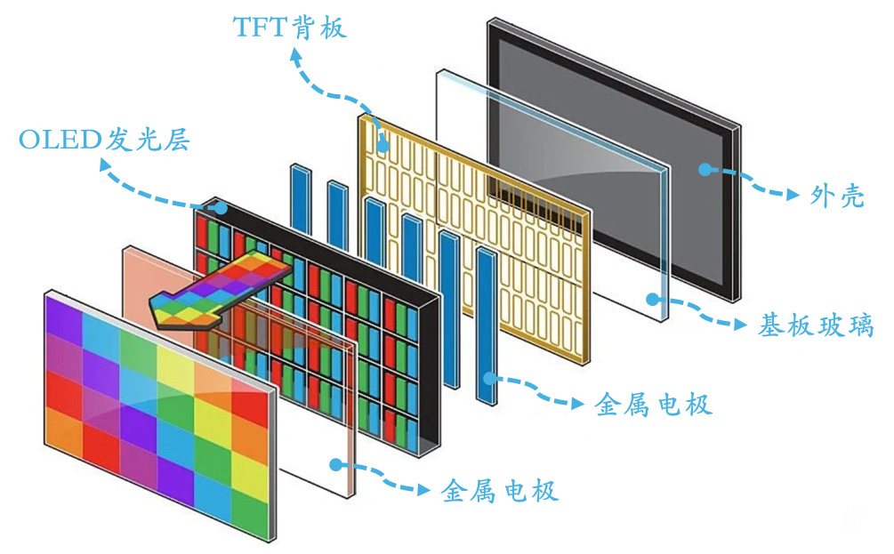
Its core structure includes an OLED light-emitting layer, TFT backplane, metal electrodes, substrate glass, and casing.
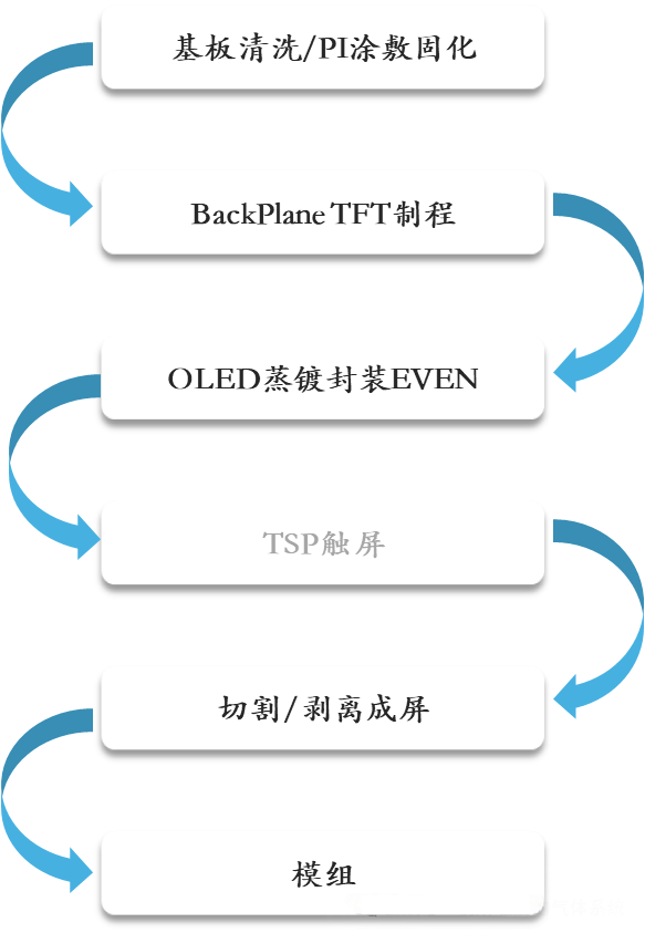
The flexible AMOLED manufacturing process encompasses key steps such as substrate cleaning/PI coating, backplane TFT preparation, OLED evaporation and encapsulation, touch module integration, laser lift-off, and module assembly.
As a company specializing in the research, development, and manufacturing of display technologies, CNK Electronics Co., Ltd.始终 stays at the forefront of technology, providing customers with diversified display solutions including OLED modules, LCD screens, and customized LCD screens.
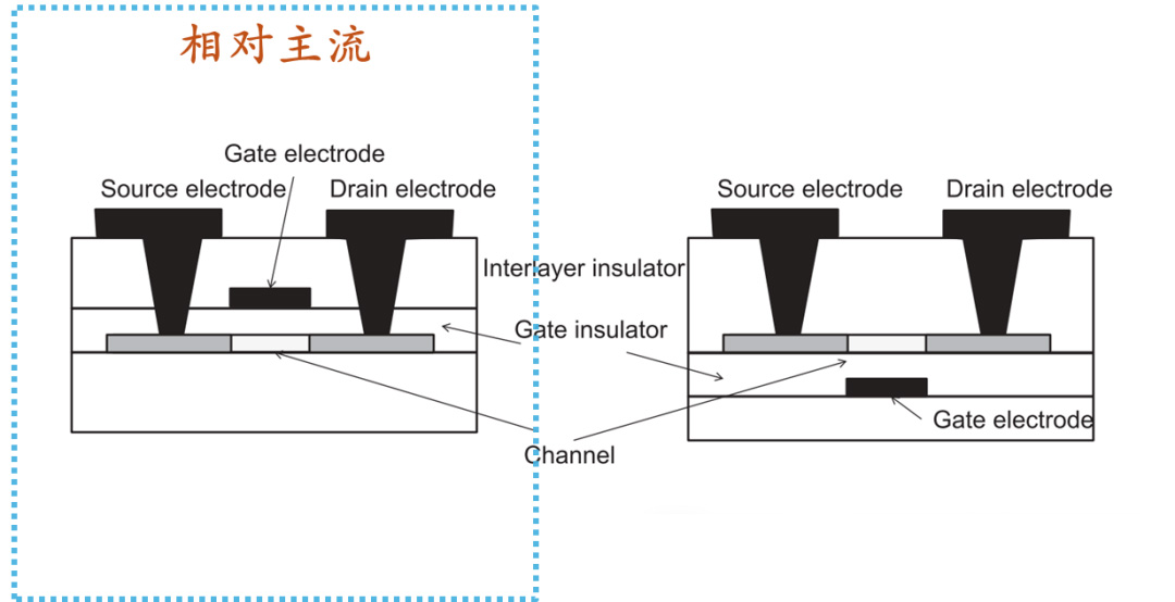
The core manufacturing process of AMOLED involves several highly technical unit processes. In the Backplane TFT (BP) process, Low-Temperature Polycrystalline Silicon (LTPS) technology has become mainstream due to its high electron mobility. Its top-gate structure process includes steps such as buffer layer deposition, channel ion implantation, laser annealing crystallization (ELA), gate metal sputtering, and source-drain implantation. Special gases play a critical role in thin film deposition, modification, and etching: for example, PECVD processes use SiH₄/N₂O/NH₃ to deposit a-Si/SiNx/SiOx thin films; Atomic Layer Deposition (ALD) employs TMA and H₂O to form Al₂O3 encapsulation layers; dry etching achieves high-precision patterning through gases such as CF4/SF6/Cl2, where BCl3 is used to reduce metal oxide layers, and Cl2 generates volatile etching products, ensuring a clean and efficient process.
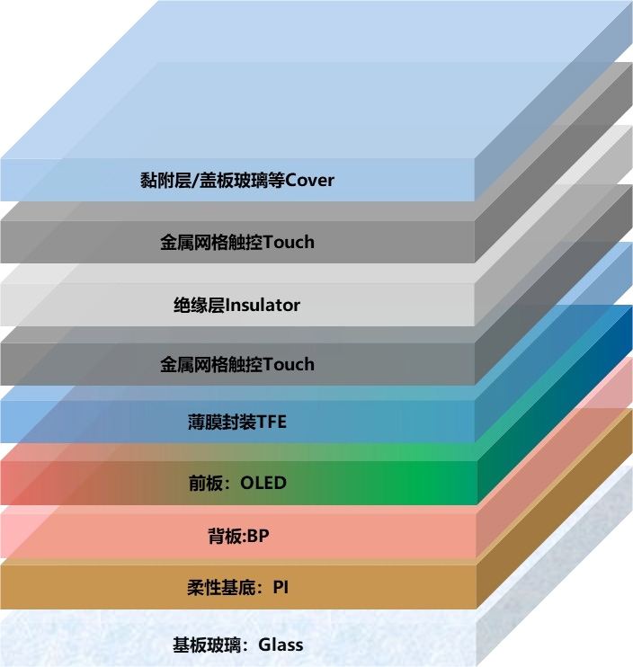
In flexible AMOLED manufacturing, laser lift-off (LLO) and thin film encapsulation (TFE) are critical to product reliability. The LLO process uses a 308nm XeCl excimer laser to separate the flexible PI substrate from the glass substrate, while TFE technology employs multilayer thin films to block moisture and oxygen, extending device lifespan.
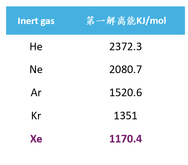
Additionally, the ion implantation (IMP) process uses BF3/PH3/H2 to provide doping atoms, with Xe serving as a neutralization gas to prevent charge accumulation.
As display technology advances toward flexibility and high resolution, the complexity and precision requirements of the AMOLED manufacturing process continue to increase. By integrating the advantages of AMOLED and LCD technologies, CNK Electronics continuously optimizes the performance and reliability of HMI human-machine interaction modules, providing innovative display solutions for consumer electronics, industrial control, and other fields.
About CNK
Founded in Shenzhen in 2010, CNK Electronics (CNK in brief) expanded the world leading factory in Longyan, Fujian in 2019. It is a specialized and innovative enterprise specializing in the design, development, production and sales of display products. CNK provides customers with a full range of cost-effective small and medium-sized display modules, solutions, and services with excellent quality worldwide. Oriented in technology and high quality, CNK keeps sustainable development, works to offer customers better and stable services.